

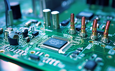
PCB fabrication refers to the process of manufacturing printed circuit boards (PCBs). It involves designing the circuit layout, transferring the design to a copper-clad board, etching away the excess copper, and drilling holes for components. The final product is a printed circuit board that serves as the foundation for electronic circuits. PCB fabrication plays a crucial role in the electronics industry, as it allows for the production of smaller, more reliable, and cost-effective electronic devices.
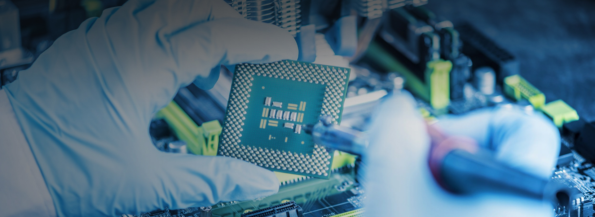
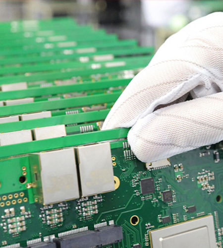
We are a Shenzhen China-based PCB PCB fabrication company with more than 20 years of experience in delivering PCB fabrication services. Our team employs advanced and innovative technologies to offer our clients top-notch PCB fabrication solutions.
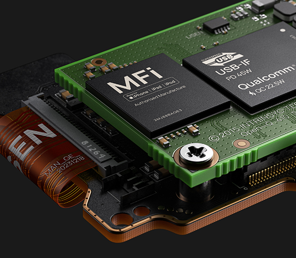
We are a team of experts specializing in high-end technological PCB fabrication services. Our services include multi-layer PCBs, rigid PCBs, flex PCBs, rigid-flex PCBs, thin/ultra-thin PCBs, high-frequency PCBs, and more. With industry-leading procedures and facilities, we deliver consistent quality, on-time, and on-budget custom PCB fabrication services throughout the China. Our dedicated team conducts thorough quality checks to ensure our products meet high standards, earning us an outstanding reputation in the market.
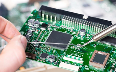
With our special techniques and equipment, we perform SMT soldering during the PCB assembly. We ensure allthe components placed during the soldering processesare not damaged and even the final soldered quality ishigher. Many times, equipment failures happened due to low-quality soldering.
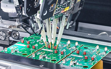
We do high quality soldering tooptimize the PCB assembly process, improve the overall equipment reliability, and adhere to the highest quality standards. We hold experience in all the SMD soldering techniques like hand soldering, hot air soldering, and hot plate soldering.
We further provide reflow soldering options for your boardas you move towards the completion of the assembly process. Get a proper reflow profile for building acceptable solder joints without causing any damage to the parts or assembly.
For the reflow soldering process, we pick the suitable machines, acceptable reflow profile, PCB component footprint design, well-designed stencils, high quality PCB, components & solder paste, and repeatable placement of surface mount components.
| Serles | Item | Spec. | |
|---|---|---|---|
| 1 | Number of layer | Standard FR4 High TG | 1-80 L (>=10 L must use High TG) |
| 2 | Product type | ATE TEST BOard | EVB、 WAT、 MLO, Prboe Card、 Load Board. Bum in Board. ESD、 SLT |
| High speed Board | M9、M8、M7、M6series | ||
| HDI | 1+N+1、 2+N+2、3+N+3、 Any-layer HDI interonnedion | ||
| High Frequency | Rogers series . Taconic series. Arlon series, Nela series. F4BK. TP series | ||
| Rigld-flex | ≤20L | ||
| FPC | ≤10L | ||
| Special Process Technology | capper matenal 、 AL matenal 、Stepped slat / Step groove 、 Embedded resistor and capacltor(Embedded R/C)、 Back drilling 、 Selective gold plating 、 POFV (Resin plug via) 、 Mixed Lamination / Hybrid Lamination | ||
| 3 | Surface Treatment | Surface Treatment | HAL,HAL/LF, Enig, Immersion Silver, Immersion Tin, OSP, ENEPIG, Plating hard gold,Gald finger (aontain segmented golden finger), Enig +OSP, Enlg +gold finger,Immersion Tin+ gold finger, Immerslon Silvert gold finger、 EPIG |
| 4 | Board thickness | Board thickness | 0.15-10.0mm |
| 5 | T/H Ratlo | 40:1 | |
| 6 | Sze | Max.Size | 610*864mm |
| 7 | Finished Copper Thidkness | Outer Layers (max) | 300Z |
| inner Layers (max) | 100Z | ||
| 8 | Line wldth/space | Min line width/space | 2.5/2.5mill |
Cutting
This process involves cutting the copper-clad board into smaller boards that can be made on the production line.
Graphic transfer
This step involves transferring the inner circuit pattern to the PCB board. This involves multiple processes such as inner layer sticking, exposure and development and etching.
Black Oxidation
This process helps to remove contaminants such as oil and impurities on the surface. It also helps to increase the specific area of the copper foil. The oxidized surface also isnt affected by moisture.
Pressing
The process of lamination involves bonding layers of circuits by means of B-stage prepeg. The discrete multilayer board is then pressed together with the adhesive sheet into the multilayer printed circuit board.
Mechanical Drilling
The use of a mechanical drill at high speed ensures through holes on the multilayer PCB.
Decontamination and sinking copper
The purpose of this process is to metallize the through hole. A three part process, this helps in decontamination, copper sinking and thickening.
Dry film and pattern plating
This process is similar to the inner layer graphics transfer as it uses photosensitive dry film to print circuit patterns on the board.
Wet film solder mask
The idea of adding the solder mask is to prevent short circuits between lines, insulation and resistance to harsh environment.
Printing
In this process, the screen for the printing plate is produced followed by printing character ink on the plate and finally drying of the ink.
Profiling
This involves separating the delivery graphics from the large panel. Many capacity parameters such as shape tolerance, inner corner size, safety distance between figure and edge of the board are considered.
Testing
Commonly used electrical testing includes needle bed test as well as flying probe test.
Immersion Tin
Electroless tin plating process uses chemical deposition to deposit tin on the PCB surface.
Final inspection
Largely this consist of the following methods: Optical Inspection – With AOI testing equipment, the machine scans the PCB and displays any defects.
Target Inspection Confirmation
This is a process of visual inspection that confirms or eliminates defects.
Visual inspection
This is menat to repair or scrap confirmed defects.
Packaging
There is a wide variety of packaging available including mositure-proof packaging, anti vibration packaging and more. Typicaly vaccum packaging is commonly used.
PCB Assembly Q&A